Tel:15324226647 Mob:+86-13930552202 Skype:Lengstech Whatsapp: +86-13930552202
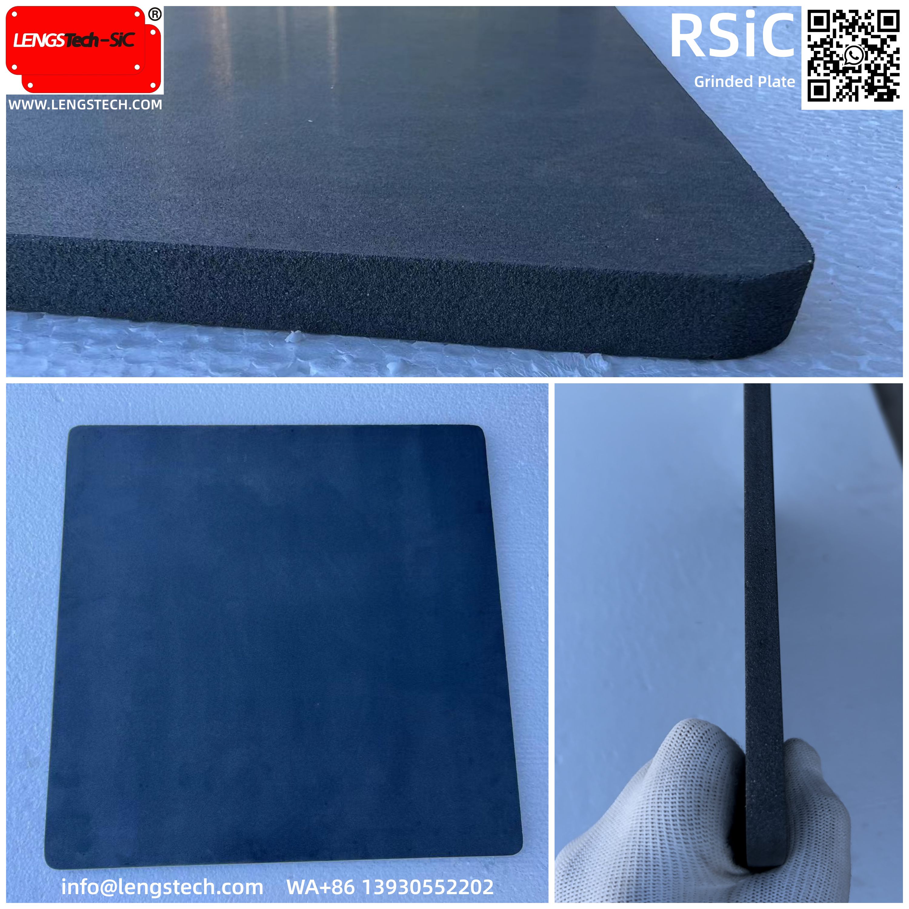
RSiC plates, featuring a purity of over 99%, no grain boundary impurities, high-temperature stability at 1650–1700℃, excellent thermal shock resistance and low creep, serve as core components for load bearing and thermal management in high-temperature film and semiconductor processes, adapting to rapid heating/cooling cycles and harsh atmospheric conditions.

High Purity & Cleanliness: SiC content ≥99%, free of grain boundary glassy phases/metal impurities, preventing film and wafer contamination for high-purity processes.
High-Temperature Stability: Sustained operation at 1650–1700℃, short-term resistance up to 1800℃, withstanding high-temperature processes such as film deposition and annealing.
Thermal Properties: High thermal conductivity, low heat storage and superior thermal shock resistance, ensuring uniform temperature, adapting to rapid thermal cycles and reducing thermal deformation.
Structural & Mechanical Performance: Low creep, high strength at high temperatures and designable porosity (10%–20%), enabling stable load bearing, high dimensional accuracy and compatibility with gas flow/exhaust requirements.
Sintering of TCO Targets & Substrates (ITO/IZO etc.): Used for high-temperature sintering (1400–1600℃) of target preforms to ensure high density and compositional uniformity, improving sputtered film quality; acts as substrate carriers in roller/tunnel kilns for continuous production, with high thermal conductivity ensuring uniform film thickness and lower edge defect rates.
Fabrication of High-Temperature Functional Films (piezoelectric/ferroelectric/dielectric): Carries substrates for 1200–1600℃ high-temperature annealing in CVD/PVD pre/post-treatment, enhancing film crystallinity and interface bonding strength; resistant to corrosion in oxygen/nitrogen atmospheres, avoiding film composition contamination.
Photovoltaic & Optoelectronic Films (PERC, perovskite etc.): Applied in high-temperature doping and passivation layer annealing of solar cells, with high dimensional stability ensuring batch production consistency; lightweight design (30%–50% lighter than traditional refractories) increases kiln loading and reduces energy consumption.
Wafer Fabrication Equipment Carrying: For 1100–1650℃ rapid thermal annealing (RTA) and post-implantation annealing in annealing furnaces, low creep and high cleanliness prevent wafer warpage and contamination, adapting to 300mm wafer mass production; serves as wafer boats/carriers in diffusion/oxidation furnaces, withstanding long-term high temperatures and oxidizing atmospheres to reduce particle contamination and improve yield; carries wafers/substrates in high-temperature deposition of CVD/PVD equipment, enabling controllable film thickness and stress via uniform heat conduction.
Power Semiconductors & Advanced Packaging: Used in high-temperature processes (e.g., pre-epitaxial treatment above 1600℃) for SiC power device chips, with excellent thermal matching to SiC materials reducing chip cracking caused by thermal stress; applied in high-temperature curing/sintering of substrates/lead frames in advanced packaging to ensure packaging reliability.
MEMS & Sensor Manufacturing: Carries micro-structural components for 1200–1500℃ high-temperature sintering/bonding, with high dimensional accuracy guaranteeing consistent mechanical and electrical performance of MEMS devices.
Selection: Select thickness (2–10mm typically) and structure (flat/grooved/porous) based on process temperature; porous plates for gas circulation, flat plates for high-precision bearing. Surface treatment (chemical cleaning/SiC coating) further reduces impurity release for ultra-high-purity processes.
Challenges & Solutions: Brittleness addressed via fillet/chamfer design, stiffener structures and optimized support points to enhance impact and load capacity; cost controlled through modular design and regeneration repair technology to extend service life.
Technological Trends: Ultra-thinning (≤3mm) and lightweight design for higher energy efficiency and productivity; precision processing (±0.02mm) to meet flatness requirements of advanced processes; composite structure development (e.g., SiC-graphite) for combined thermal conductivity and thermal shock resistance, expanding applications in short-term processes above 1700℃.
The core value of RSiC plates in high-temperature film and semiconductor sectors lies in the integrated performance of high-temperature stability, cleanliness and efficient thermal management. As a critical consumable for high-end target manufacturing, advanced wafer processing and precision film preparation, its application scenarios are continuously expanding with the development of third-generation semiconductors and new display technologies.
Tel:15324226647
Mobile:+86-13930552202
E-mail: info@lengstech.com
Skype: Lengstech
Whatsapp: +86-13930552202


Copyright 2026 © Tangshan LENGS Technology Co., Ltd. All Rights Reserved.